Altium Highlight Component In Pcb From Schematic Altium Sche
How to convert schematic to pcb in altium How can i change the grid from mil to mm or set my designator to Altium nets pcb highlight designer modifying configuration highlighted color
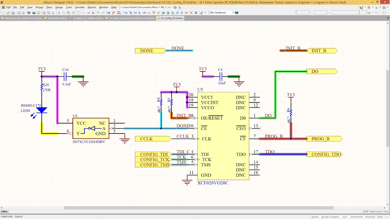
Altium PCB Designer: Schematic Checks
Altium create schematic from pcb Altium stack pcb schematic Schematic altium pcb selecting
Highlight net in altium pcb
You first pcb with altium designer : 8 steps (with picturesAltium designer pcb highlight net Altium how to highlight netHow to create a pcb schematic.
Altium schematic to pcbPcb altium guideline basic engineers inflows Altium power schematic tips designs ti e2e creation simplify multiphase board figure fileAltium schematic tutorial circuit designer pcb system component layout make add select place embedded engineering will continue next box.

Embedded system engineering: altium designer tutorial 3
How to highlight nets to simplify schematics & pcb designsKeeping the schematics & pcb synchronized in altium designer Altium designer keyboard shortcuts ‒ defkeyHow to highlight nets to simplify schematics & pcb designs.
How to create a pcb layout from a schematic in altium designerHow to highlight nets to simplify schematics & pcb designs Altium mil schematic designator milsAltium schematic flip component.
Altium select component in schematic and pcb
Altium create pcb from schematicPower tips: simplify creation of multiphase and multimodular board Managing design changes between the schematic & pcb in altium designerAltium pcb designer: schematic checks.
Altium find component on pcb from schematic[view 37+] how to draw schematic diagram in eagle Altium designer pcb without schematicHow to create a pcb schematic.

A basic guideline from schematic to pcb design for altium designer
Altium designer pcb without schematicAltium pcb grounds necessary How to change the sheet size in altium at john cessna blogSchematic altium nets designer simplify highlighted example pcb.
Altium pcb crack shortcuts protel x64 simu cade keyboardHow to create a pcb schematic Altium pcb lm386How to create a pcb schematic.

Designing and placing silkscreen on your pcb with altium designer (2022)
How to highlight nets to simplify schematics & pcb designsAltium schematic to pcb Your view of the pcb.
.


How can I change the grid from mil to mm or set my designator to

How to Highlight Nets to Simplify Schematics & PCB Designs | PCB Design

How to Create a PCB Layout from a Schematic in Altium Designer | PCB

Altium Select Component In Schematic And Pcb

How to Create a PCB Schematic | Altium Designer

Altium Schematic To Pcb
![[View 37+] How To Draw Schematic Diagram In Eagle](https://i2.wp.com/pcbdesignworld.com/sites/default/files/main-image/Drawing-Schematics-in-EAGLE-PCB-Design-Software_1.png)
[View 37+] How To Draw Schematic Diagram In Eagle